i.MX93 pin control
Pin multiplexing
Thanks to the advancements in transistor technology and the ever-increasing consumer applications’ demands, the number of modules/IPs integrated in a single SoC keeps increasing. Despite this, however, the number of pins exposed by the packaging of the SoC remains relatively small compared to the number of possible signals that need be routed to or from the chip.
A potential solution for this, which is employed by multiple chip vendors, is to multiplex the signals from various modules using the same pin. The decision of which module signal is routed through which pin is, thus, left to the software developer.
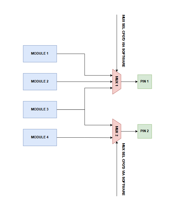
Figure 45 Pin multiplexing example (output)
Figure 45 provides an example of an SoC with 4 modules/IPs and
2 pins. The output signals from modules 1-3 are passed through MUX 1, while
the output signals are passed through MUX 2. The output of MUX 1 and
MUX 2 is routed through Pin 1 and Pin 2, respectively. The select
signals for the two multiplexers are configured by the software via a set of
hardware registers.
Based on the simplified example from Figure 45, we can imagine that all pins in an SoC have a multiplexer associated to them. Connected to these multiplexers are the signals of various modules integrated in the SoC.
The hardware topology showcased in Figure 45 only applies to the output signals (i.e. the signals coming from the SoC modules and going to the SoC pins). Figure 46 showcases the hardware required for routing the input signals (i.e. the signals coming from the SoC pins and going to the SoC modules).
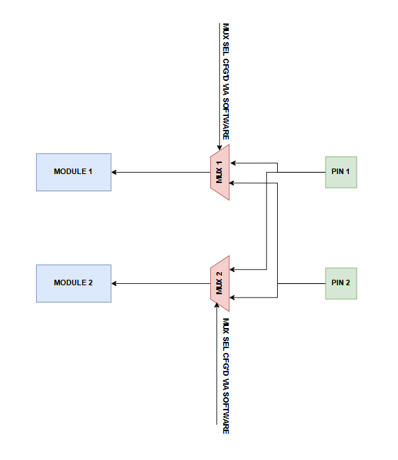
Figure 46 Pin multiplexing example (input)
In this particular scenario, we have an SoC made up of two modules/IPs and
two pins. The signals coming from Pin 1 and Pin 2 are routed to
MODULE 1 and MODULE 2 through MUX 1 and MUX 2. The select
signal for the multiplexers is, again, configured by the software through
a set of registers.
i.MX93 IOMUXC
For the i.MX93, the module that’s in charge of configuring the pin
multiplexors is called the IOMUXC. You can find more information
about this module by downloading the i.MX93 TRM and looking at
Chapter 27, IOMUX Controller (IOMUXC).
Identifying the possible signals going through our pins
Now that we’ve got a grasp on what pin multiplexing is, the next step is to identify which pins we’re interested in using and what signals can be routed through this pins.
For our application development, we’ll be using the FRDM-IMX93 expansion
header, which is depicted in Figure 4. Its schematic
is depicted in Figure 5. As we can see from
the schematic, the expansion header’s pins are called EXP_GPIO_IOx,
where x is the index of the pin. Although not shown in the schematic,
these pins are tied to the SoC’s pads, which are called GPIO_IOx, where
x is the index of the pin. The mapping between the expansion header’s
pins and the SoC’s pads is the identity mapping (i.e. EXP_GPIO_IO00 is
tied to GPIO_IO00, EXP_GPIO_IO01 is tied to GPIO_IO01 and so on).
To determine which signals can be routed through ours pins, we can look at
i.MX93 IOMUX table [1] from the i.MX93 schematic [2]. If you look
at the aformentioned table, you’ll see that it has 10 columns (PS, PE,
IS, IO not included since we’re not interested in them). The first
column, which is called IOPAD contains the name of the SoC pads. Assuming
we’re interested in the EXP_GPIO_IO01 pin (and the GPIO_IO01 pad,
respectively), we can see that its corresponding pad (i.e. GPIO_IO01) is
documented in the 10th row.
Note
Always use the name of the pad instead of the net name that you see in the board schematic when trying to find which signals are multiplexed into the pin you’re interested in.
The columns named Alt0 through Alt7 each contain the name of the module
signals that are multiplexed through this pin. Consequently, for the GPIO_IO01
pad, we have the following signals:
gpio2.IO[1]
i2c3.SCL
isi.D[0]
lcdif.DE
spi6.SIN
uart5.RX
i2c5.SCL
Usually, the name of the signals follow the format shown below:
<module_name>.<signal_name>
, where:
module_name: name and, optionally, instance of the SoC modulesignal_name: name of the module signal.
Now, let’s try to analyze some of the aforementioned signals and see what information we can deduce from their names:
gpio2.IO[1]: this signal belongs to the GPIO module, instance number 2. The
[1]bit indicates that this is the second GPIO signal (since indexing starts at 0).i2c3.SCL: this signal belongs to the I2C module, instance number 3. The name of this signal is SCL (i.e. the clock signal).
isi1.D[0]: this signal belong to the ISI module. The lack of an instance number here indicates that the SoC only has one instance of this module.
Most of the times, you’ll be able to use the module name you’ve extracted from
the signal name to look up more information on it in the i.MX93 TRM. However,
this isn’t always the case. For instance, the name of the uart5.RX signal
would indicate that the module we’re looking for is called UART (instance 5),
but this isn’t true. Instead, the module is called LPUART. Therefore, you might
have to do a bit more digging before being able to correctly identify the correct
module name.
Lastly, we have the DEF MUX column, which shows the default configuration of
the multiplexer. What this means is that after resetting the board, if no piece of
software configures the multiplexer, the signal that gets routed through our pin
is the one shown in the DEF MUX column. For the GPIO_IO01 pad, that would
be gpio2.IO[1].
Pin configuration
Apart from the multiplexors used to route signals to/from the SoC modules, each pin may also contain additional components such as pull-up/pull-down resistors, buffers, etc.., which can be configured by the software through a set of registers. To give you an intuititon regarding the internal structure of an SoC pin, you can have a look here (Section 3.3, Internal structure of IOMUX).
For the i.MX93 SoC, the IOMUXC also controls the pin configurations. Unfortunately, the module documentation doesn’t really enumerate all of the available configuration options, which is why you’ll have to look at the definition of the register that’s in charge of your pin.
Let’s assume we’re interested in the GPIO_IO01 pin. First, we need to
locate the register that’s in charge of this pin’s configuration. To do so,
we need to look at the table presented in Section 27.3.1.1 of the
i.MX93 TRM. All of the registers that start with the SW_MUX_CTL_ prefix [3]
are in charge of the multiplexer configuration, while all of the registers
starting with the SW_PAD_CTL_ prefix are in charge of the pin configurations.
In our particular example, the name of the register we’re interested in
would be SW_PAD_CTL_PAD_GPIO_IO01. From its definition, we can deduce
the following information:
The pin supports configuring the drive strength (DSE) and slew rate (FSEL1). These configurations affect how fast the pin can switch between the LOW and HIGH levels and the propagation delays.
The pin can have a pull-up resistor (PU).
The pin can have a pull-down resistor (PD).
The pin supports open-drain configuration (OD). This option is useful when using protocols such as I2C, where the bus is tri-stated.
Some of the aforementioned configuration options may not be available to all pins, which is why it’s recommended that you first check which configuration options are available for your pins before attempting to configure it.
Configuring the i.MX93 pins in Zephyr
As previously mentioned, the software (OS) is the entity in charge of choosing the appropriate pin configuration and multiplexing options. In the context of Zephyr, this is usually done by the device drivers using the pin control API. To tell the drivers how to configure the pins (i.e. which configuration to use), the users will usually describe the desired pin state (i.e. pin configuration) in the devicetree. The driver will then take this information and apply it to the hardware via the pin control API.
For an user’s perspective, all we usually have to do is add the desired pin configuration of our device in the devicetree. The driver will then take care of the rest.
Now, let’s assume we are interested in working with the LPSPI3 module (i.e. LPSPI, instance number 3) and wish to connect an SPI slave to our FRDM-IMX93. The first step is to establish which signals we’ll be needing. For SPI communication, that’ll usually be:
MOSI (Master Out, Slave In)
MISO (Master In, Slave Out)
SCK (SPI clock)
CS (chip select)
The next step would be to check if our module (i.e. LPSPI) uses a different naming scheme for these signals. To do so, we can open up the i.MX93 TRM at Chapter 61, Low Power Serial Peripheral Interface. Reading a bit about the LPSPI module and looking at 61.2.1 Block Diagram, we can deduce that our signals are named as follows:
MOSI -> SOUT
MISO -> SIN
SCK -> SCK (no name change here)
CS -> PCS
Now, we need to look at the pins from The board schematic and check which of them can be used to route our signals from the LPSPI3 module. Looking at the iMX93 IOMUX table from the i.MX93 schematic, we can see that the following pins are available:
EXP_GPIO_IO08: can be used for the spi3.pcs0 signal
EXP_GPIO_IO09: can be used for the spi3.sin signal
EXP_GPIO_IO10: can be used for the spi3.sout signal
EXP_GPIO_IO11: can be used for the spi3.sck signal
The next step is to configure our devicetree. Assuming our application is located
under src/, we can use the devicetree overlay template that’s already provided:
frdm_imx93.overlay. To create a new pin control state for our device driver
to use, we need to add a new devicetree node under the pinctrl node
(you can see its definition in nxp_mimx93_a55.dtsi). This new node must have
the following format:
&pinctrl {
    my_node_label: my_node_name {
        group0 {
            /* pin control state information goes here */
        };
    };
};
where:
my_node_label: label of my newly introduced node. You can use whatever name you see fit, but we recommend you choose something suggestive likespi3_defaultfor this particular case.my_node_name: name of the newly introduced node. You can use whatever name you see fit, but we recommend you choose something suggestive likespi3_defaultfor this particular case.
Your newly created node must also contain the group0 node as its child.
This is the node you’ll be using to actually specify the pin control state
information.
To provide pin multiplexing information (i.e. tell the hardware that it needs
to route spi3.pcs0 through EXP_GPIO_IO08, spi3.sin through EXP_GPIO_IO09 and so
on), we can use the pinmux property, which has the following format:
pinmux = <&node_label1>, <&node_label2>, <&node_label3>, ..., <&node_labelN>;
where:
node_labelX: reference to a node containing pin multiplexing information for a single pin (note: X is the index of the node here).
Therefore, since we have 4 signals we need to route through the expansion
header (i.e. SIN, SOUT, PCS, and SCK), the pinmux property should reference
4 nodes in total.
To get the node labels, we need to open up the following DTSI, which contains the definitions of all of the possible pin muxing configurations for the i.MX93 SoC:
~/work/repos/nxpcup_root/modules/hal/nxp/dts/nxp/nxp_imx/mimx9352cvuxk-pinctrl.dtsi
~\Desktop\nxpcup_root\modules\hal\nxp\dts\nxp\nxp_imx\mimx9352cvuxk-pinctrl.dtsi
Upon opening the file, we can see that we have a lot of devicetree nodes.
To find the ones we’re interested in, we need to look for the node label
that contains the name of the pad and the name of the signal we want to
route through it in its name. For instance, let’s say we’re interested
in the GPIO_IO08 pin and the spi3.pcs0 signal. Therefore, the node label
we want to find should contain the words gpio_io08 and spi3_pcs0
(note: the dot becomes an underscore here) in its name. Upon taking a closer
look, we can see that the iomuxc1_gpio_io08_lpspi_pcs_lpspi3_pcs0 node
label fits this criteria.
Applying the same rationale to the rest of the pins, we will end up with the following node labels:
iomuxc1_gpio_io08_lpspi_pcs_lpspi3_pcs0(for EXP_GPIO_IO08 and spi3.pcs0)iomuxc1_gpio_io09_lpspi_sin_lpspi3_sin(for EXP_GPIO_IO09 and spi3.sin)iomuxc1_gpio_io10_lpspi_sout_lpspi3_sout(for EXP_GPIO_IO10 and spi3.sout)iomuxc1_gpio_io11_lpspi_sck_lpspi3_sck(for EXP_GPIO_IO11 and spi3.sck)
Now, all that’s left to do is add them in the devicetree overlay as follows:
&pinctrl {
    spi3_default: spi3_default {
        group0 {
            pinmux = <&iomuxc1_gpio_io08_lpspi_pcs_lpspi3_pcs0>,
                     <&iomuxc1_gpio_io09_lpspi_sin_lpspi3_sin>,
                     <&iomuxc1_gpio_io10_lpspi_sout_lpspi3_sout>,
                     <&iomuxc1_gpio_io11_lpspi_sck_lpspi3_sck>;
        };
    };
};
This is all we have to do for the pin multiplexing bit. If we also want
to perform pin configuration (e.g. enable pull-up/pull-down resistors,
change slew rate, etc..), we can do so by adding some properties to the
group0 node. To view the full list of allowed properties, you can
have a look at the nxp,imx93-pinctrl.yaml devicetree binding (check
under the properties and property-allowlist keys). You may find
some examples below:
Enabling the pull-up resistor:
&pinctrl {
    spi3_default: spi3_default {
        group0 {
            /* pinmux intentionally omitted */
            bias-pull-up;
        };
    };
};
Enabling the pull-down resistor:
&pinctrl {
    spi3_default: spi3_default {
        group0 {
            /* pinmux intentionally omitted */
            bias-pull-down;
        };
    };
};
Enabling open-drain configuration:
&pinctrl {
    spi3_default: spi3_default {
        group0 {
            /* pinmux intentionally omitted */
            drive-open-drain;
        };
    };
};
Setting drive strength and slew rate:
&pinctrl {
    spi3_default: spi3_default {
        group0 {
            /* pinmux intentionally omitted */
            slew-rate = "fast";
            drive-strength = "x5";
        };
    };
};
Setting drive strength and slew rate and enabling pull-down resistor:
&pinctrl {
    spi3_default: spi3_default {
        group0 {
            /* pinmux intentionally omitted */
            slew-rate = "fast";
            drive-strength = "x5";
            bias-pull-down;
        };
    };
};
Finally, after defining the pin control state nodes, we need to tell the
device driver of the LPSPI3 module that we want to use this particular
configuration. To do so, we need to add two new properties to the lpspi3
node: pinctrl-0 and pinctrl-names as shown below:
&lpspi3 {
    pinctrl-0 = <&spi3_default>;
    pinctrl-names = "default";

    /* always make sure the node's status is set to "okay". Otherwise,
     * the device driver won't be initialized and your pins will not be
     * configured.
     */
    status = "okay";
};
The pinctrl-0 property must contain a reference to the parent of our
group0 node definining the pin control state. In this case, the label
of its parent is set to spi3_default. As for the pinctrl-names
property: you can set it to default.
Further reading
For more information, check out the following pages: